
Smart Semiconductor Manufacturing factory to Improve Operational
Semiconductor Industry Outlook & Trends
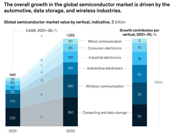
Over the long run, semiconductor revenues are likely to oscillate around a trend line. Still, that trend line looks steeper than ever before as we enter a period of robust secular growth.
The global semiconductor chip industry is expected to grow 10% in 2022 to over US$600 billion for the first time ever. Chips will be even more important across all industries, driven by increasing semiconductor content in everything from cars to appliances to factories, in addition to the usual suspects—computers, data centers, and phones.

In today’s increasingly complex, geographically dispersed, and constantly changing global marketplace, semiconductor manufacturers must innovate to meet the demand for unstinting quality with higher efficiency and lower cost. Increased visibility and greater collaboration across supply chain networks are essential to their ability to adapt processes to respond effectively to rapid and frequently volatile change. Since flexible technologies are essential to meeting these requirements, semiconductor MES has become a fundamental element in the technology strategy of semiconductor manufacturers.
AI / ML has significant value-creation potential in the semiconductor industry. They can reduce costs, improve yields and increase a fab’s throughput.
Besides, through this powerful combination, factories can capture productivity gains of 30% to 50% for direct labor and 10% to 20% for maintenance productivity. There is an average improvement of 10-15 %in overall equipment effectiveness, increases of 1% to 3% in yield, and a 30% to 50% decrease in customer complaints. The total experience is enhanced multifold by implementing Industry 4.0 in the semiconductor industry.
Industry 4.0 brings with it superior automation and automated decision-making, which result in faster responses to production needs and enhanced efficiency
McKinsey analysis based on a range of macro economic assumptions suggests the industry’s aggregate annual growth could average from 6 to 8 percent a year up to 2030. Supply chain & chip shortages issues to remain front and center, possibly well into 2023.
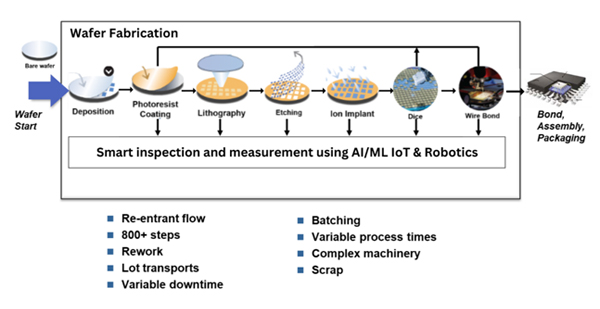
7 crucial steps in semiconductor manufacturing
A semiconductor chip is an electric circuit built up in a series of nanofabrication processes performed on the surface of substrates (wafers) composed of highly pure single-crystal silicon. The production of a microchip involves adding impurities to the base element in a process called “doping” to adjust the conductance or inductance of the outcome, based on the type and intensity of impurities added. Here are the seven crucial steps involved in the manufacturing of semiconductors.
• Cleaning
Silicon wafers forming the base of the microchip are cleaned by a solvent and followed by a deionized water (DI) rinse and blow-dry. This is the first and most crucial step of semiconductor manufacturing, as even slight contamination can cause defects in the circuit. Generally, chemical agents remove the contamination, varying from ultra-fine particles to minute amounts of metallic residues generated during the production process or natural oxide layer formed due to air exposure. The final wafer cleaning step involves a Hydrofluoric Acid dip for two minutes to remove the silicon oxide layer. Then, the wafer is put under running DI water, and a wettability test is conducted to confirm whether the cleaning was successful or needed more. If the water turns into little beads and rolls off, then the wafers are considered good to go for further processing.
• Deposition / Oxidation:
The semiconductor chip manufacturing process initiates with a silicon wafer. Wafers are sliced from a silicon bar made of 99.99% pure silicon and polished until they become highly smooth. Depending on the type of structure being created, thin films of dielectric (insulating) and metal (conducting) materials are deposited on the wafer surface to build a microchip. This process is known as a deposition. There are multiple ways to perform deposition: sputtering, electro deposition, chemical vapor deposition, and thermal deposition. The kind of technique used for deposition depends upon the process node, type of chip, and the amount of time needed to do the deposition.
The role of the oxidation process is to form a protective film on the surface of the wafer. It can protect the wafer from chemical impurities, prevent leakage current from entering the circuit, diffusion during ion implantation, and the wafer from slipping off during etching.
The first step of the oxidation process is to remove impurities and pollutants, such as organic matter, metals, and evaporation residual moisture with four steps. After the cleaning is completed, the wafer can be placed in a high temperature environment of 800 to 1200 degrees Celsius, and a layer of silicon dioxide is formed by the flow of oxygen or vapor on the wafer surface. Oxygen diffuses through the oxide layer and reacts with silicon to form oxide layers of different thicknesses, which can be measured after the oxidation is complete.
Sputtering involves the bombarding of ions on the target materials, which knocks off atoms and molecules that are further deposited on the wafer surface. Electrodeposition is used to form copper wire layers. In contrast, chemical vapor deposition includes special gases that cause a chemical reaction to generate molecules that are then deposited on the wafer surface to form a film. Thermal oxidation includes heating up of wafer to form a silicon oxide film on the wafer surface.
In addition to the oxidizer, there are other variables that affect the thickness of the silicon dioxide layer. First of all, the wafer structure, surface defects, and internal doping concentration will affect the rate of formation of the oxide layer. In addition, the higher the pressure and temperature generated by the oxidation equipment, the faster the oxide layer will be formed. In the oxidation process, it is also necessary to use dummy wafers according to the location of the wafers in the unit to protect the wafers and reduce the difference in oxidation degree.
• Photoresist coating
Photomask is the use of light to “print” circuit patterns onto a wafer. We can understand it as semiconductor parts drawing on the surface of the wafer. The higher the fineness of the circuit pattern, the higher the integration of the product chip, which can only be achieved through advanced photomask technology.
The first step in drawing a circuit on a wafer is to coat photoresist on the oxide layer. Photoresist changes the chemical properties of the wafer to become “photographic paper”. The thinner the photoresist layer on the surface of the wafer, the more uniform the coating, and the finer the patterns that can be printed. In addition, this step can use the “spin coating” method.
According to the difference of UV light reactivity, photoresist can be divided into two types: positive glue and negative glue. The former will decompose and disappear after being exposed to light, leaving a pattern of unreceived areas, while the latter will polymerize after being exposed to light to let the pattern of the light-receiving part appear.
The semiconductor wafer is covered with a light-sensitive coating called ‘photoresist’ or ‘resist’ that blocks everything not meant to be exposed to ultraviolet light. The resist coating can be positive or negative, depending upon the chemical structure of the material and the way that the resist reacts with light. With positive resist, the area exposed to light changes its structure, whereas with negative resist, the areas hit by light polymerize and become more difficult to dissolve. Generally, a positive resist is used in semiconductor manufacturing due to its higher resolution capabilities. It is crucial to have a resist coating method to have a uniform coating of photoresist over the surface of the substrate. Several options available for resist coating include spin coating, spray coating, dip Photomask is the use of light to “print” circuit patterns onto a wafer. Specifically, it can be divided into three steps: photoresist coating, exposure and development.coating, inkjet printing, and slot-die coating.
• Lithography
Lithography is a crucial step in the chipmaking process which involves transferring patterns of geometric shapes in a mask to a thin layer of radiation-sensitive material called resist. This process determines just how small the transistors on the chips can be. The geometric shapes and patterns on a semiconductor make up the complex structures that allow dopants to complete a circuit to fulfill a technological purpose. During this process, the semiconductor wafer is inserted into a lithography machine, where it is exposed to deep UV lights to produce the finest details of a chip. The light projected through the ‘reticle’ causes a chemical change that enables the pattern to be replicated on the resist. A complementary metal-oxide-semiconductor (CMOS) wafer can undergo the photolithographic cycles as many as 50 times.
• Development
The step after exposure is to spray developer on the wafer, in order to remove the photoresist in the area not covered by the pattern so that the printed circuit pattern can be revealed. After the development is completed, it needs to be checked by various measuring equipment and optical microscopes to ensure the quality of the drawing of the circuit diagram. During the exposure process, the finer the printed pattern, the more components can be accommodated in the final chip, which helps to improve production efficiency and reduce the cost of individual components.
• Etching
After the photo lithography of the circuit diagram is completed on the wafer, an etching process is used to remove any excess oxide film and only the semiconductor circuit diagram is left. To do this, liquid, gas or plasma is used to remove the unselected parts.
There are two main etching methods, depending on the material used: wet etching that uses a specific chemical solution for chemical reaction to remove the oxide film, and dry etching that uses gas or plasma.
1) Wet Etching
Wet etching that uses chemical solutions to remove oxide films has the advantages of low cost, fast etching speed, and high productivity. However, wet etching has the characteristics of isotropy, that is, its speed is the same in any direction. This will cause the mask (or sensitive film) and the etched oxide film to not be completely aligned, making it difficult to process very fine circuit diagrams.
2) Dry Etching
Dry etching can be divided into three different types:
The first is chemical etching, which uses etching gas (mainly hydrogen fluoride). Like wet etching, this method is also isotropic, which means that it is not suitable for fine etching.
The second method is physical sputtering, that is, ions in the plasma are used to strike and remove the excess oxide layer. As an anisotropic etching method, it has different etching speeds in the horizontal and vertical directions, so its fineness must exceed that of chemical etching. However, the disadvantage of this method is that the etching speed is slow, because it completely relies on the physical reaction caused by ion collision.
The third method is reactive ion etching (RIE). It combines the first two methods, that is, while using plasma for ionized physical etching, and chemical etching is performed with free radicals generated after plasma activation. In addition to the etching speed exceeding the first two methods, RIE can use the characteristics of ion anisotropy to achieve high-definition pattern etching.
• Ion Implantation
This step involves the implantation of impurities to provide the silicon substrate semiconducting properties. Generally, impurities such as phosphor, arsenic, or boron are implanted in the wafers that are shot into the wafer in a bullet-like fashion. Sacrificial films prevent the ions from being shot at the unwanted places of the wafer. Directing electrically charged ions (positive or negative) into the silicon crystal controls the flow of electricity and allows the creation of transistors. After this procedure, the remaining sections of resist are not etched or ionized.
• Packaging
Packaging is a crucial part of semiconductor manufacturing and design as it can affect the power, performance, and cost on a macro level and functionality on a micro level. The semiconductor wafer is sliced and diced with a diamond saw to get the individual chips out of the wafer. Semiconductor chips are cut from the wafer and are referred to as ‘dies,’ which can vary in different sizes. The chip die is placed into a substrate, a type of baseboard that uses metal foils to direct the input and output signals of a chip to other parts of the system. A heat spreader is placed on the top of the lid to ensure that the microchip stays cool during operation.
The microchip becomes ready to be used in electronic equipment such as smartphones, TV, tablets, or other devices. Although the semiconductor’s size is less than a thumb, one chip can contain billions of transistors that power up your device.
Challenges with Semiconductor chips manufacturers
Semicon manufacturing is unquestionably one of the most complex and sensitive manufacturing processes in the world. Creating line widths on silicon wafers down to five nanometers or less with billions of transistors means that even the smallest vibration or misalignment during fabrication will cause issues.
- Frequent design changes due to unstable processes and machinery and long lead time ( about 2 months) will make it difficult to maximize the fab performance.
- Alongside the sophisticated processes required to manufacture, the industry is further challenged with very short product life cycles involving millions of devices, or, the need for small batches of niche products to be produced over decades
- Incredibly expensive equipment such as extreme ultraviolet (EUV) scanners costing over $125 million each combined with the need for costly clean room real estate truly makes IC manufacturing one of the most challenging business environments.
- Production yield issues: It affects output per unit of input resources, waste generation, environmental and financial sustainability, time to market, and costs
- Master Data Management: Maintainability and Change Control are two key elements of Master Data Management.
- Market Readiness: Keeping pace with technological developments, build robust and secured chipsets supporting new ageconnectivities and sensors interoperability in place
- Pre and Post Silicon Validation:Focusing on optimized designs and error-free performance by developing test applications, functional validation, throughput testing, power and CPU usage optimization
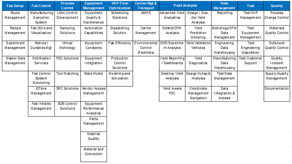
Component Business Model for the Fab
Why Manufacturing 4.O for the Semiconductor Industry?
- Digital Transformation
The objective of any MES system is to offer as much out-of-box support as possible, and to map and control physical and business processes. Manufacturing 4.0 is a modular system covering a wide range of functionality including advanced planning and scheduling; tracking of materials, equipment, and durables; management of quality processes such as exception management, sampling, experiment management, document management and SPC. The system ensures efficiency through labor management, maintenance management, costing and warehouse. Modules are preintegrated and have extensive configuration options.
MES drives value through machine-efficiency, error-proofing the production from raw materials to finished goods.
- Ensure connectivity and full Autonomous production
Semiconductor chip manufacturing plants include a variety of process, metrology, material handling (storage, sorting and transport) equipment from different vendors. Full automation and complicated process controls of the semiconductor manufacturing process requires integration of multiple domain specific applications. (e.g. Real-time dispatching, equipment interface programs, material handling systems, advanced process control, statistical process control, recipe management systems, etc)
Manufacturing 4.0 resolves the challenges of bidirectional connectivity over a diversified set of communication protocols, with the ability to design, deploy and monitor automation workflows, plus supporting the addition of specific drivers for each protocol. Beyond the connectivity, the solution encompasses a factory automation module that orchestrates different physical and logical systems such as automatic transport systems, ensuring full automation
- Execute advanced Industry 4.0 scenarios
Through connectivity and IoT integration, MES provides a unique factory digital twin, fabLIVE. Advanced mobile experience offers context specific UIs adaptable to different formats. Augmented reality (AR) can show any operator, equipment or product data from across the MES superimposed over a live camera image on any smartphone, tablet, or AR headset
Industry 4.0 brings with it superior automation and automated decision making, which result in faster responses to production needs and enhanced efficiency.
- Ensure visibility and analytics
Manufacturing 4.0 provides a complete set of visibility and analytics solutions, including a built-in query builder, a wide range set of out-of-the-box reports, standard or user-generated dashboards with KPIs or real time data and pre-built data warehouse cubes for slicing and dicing operations. The IoT Data platform is a highly scalable platform that combines IoT data with contextual intelligence from MES to help manufacturers identify actionable insights to improve performance, efficiency, and innovation.
- Deploy easily on cloud, on-prem or hybrid
MES offers cloud, on-prem or hybrid infrastructures. The solution reliably deploys complete or updated software, dependencies, customization, and master-data from your CoE to multiple plants from a single DevOps open platform
- Digital Twin functionality
To handle the current complexities of whole manufacturing operations in semiconductor manufacturers, legacy systems don’t have enough capability for decision making. Complexity of optimization of multiple fabs operations due to increase of the number of fabs. Dynamic variations caused by market demands, frequent engineering change, shorter technology life cycle Enterprise perspective manufacturing application and data platform to optimize entire fab operations, Digital Twin, have become more and more important
- Improve quality management and control
MES drives value through machine-efficiency, error-proofing the production from raw materials to finished goods. Semiconductor MES is focused on the proactive improvement of processes, such as preventing quality problems rather than reacting to them. Advanced systems are also designed for integration to accommodate the multi-tiered ecosystem of modern device manufacturing, in which many companies are fabless and must work seamlessly with subcontractors.
- Empowering the Workforce
The semiconductor industry faces a skilled labor shortage. Critical Manufacturing MES provides guidance and support for employee training through intuitive, user-configured work instructions, reports, dashboards, and interactive technologies. It empowers process owners, allowing them to configure the system and to create and build GUIs and workflows themselves to support their tasks fully
- Predictive maintenance for increased uptime
Manufacturing 4.0 also improves yields through on-time predictive maintenance of machines and components, avoiding potential breakdowns and efficiency losses. Data from each machine and its components can be monitored through an AI/ML-powered system that learns and improves maintenance schedules over time. In addition, these systems can automatically alert required users and suggest actions to keep the system running at maximum efficiency through a centralized dashboard. Manufacturers can use such systems to predict the working life and utilization rate of dies, tools, sensors, and the overall equipment effectiveness based on historical data and industry benchmarks.
- MES for Semiconductor Supply Chain
Ideally, a single MES platform can serve the entire processing lifecycle to support better traceability, as customers demand. Traditionally, MES for the fab was not suited to serve back-end assembly and test, and R&D and silicon needed different systems too. With Manufacturing 4.0, it’s possible to choose one supplier, one platform, to serve all of these. A single MES can streamline the IT landscape and improve data flows.
Advanced Semiconductor Scenarios
Master data management
Each product in a fab can require the tracking of thousands of pieces of information about process flow, recipes, parameters, reticles, specifications and sampling, to name a few. A modern MES must have the ability to readily maintain and control these huge volumes of data and provide a complete material history for the final product with full change management and versioning control. It must offer the flexibility to handle common sub-flows with the changes that are made for each layer and provide mechanisms to re-use complete flow blocks while defining appropriate context(e.g.: layer number) so that the different process elements can be resolved correctly.
Automatic validation prior to processing
There may be hundreds or even 1,000+ process steps to produce a given semiconductor product, throughout which everything needs to be tracked and checks carried out to ensure there is no misprocessing. Automatic validation prior to processing reduces the risk of errors by validating whether the right product is on the right tool, with the correct recipe and right durable, and the operator has the correct training and authorization.
Multi-chamber tools
Cluster tools have multiple chambers which can run processes in parallel or sequentially, offering significant efficiencies. Tool vendors typically offer different running modes for maximum efficiency, chamber dedication or some engineering use cases. However, these tools require proper modeling and special control logic in the MES to fully take advantage of the complex capabilities. As an example, if any of the chambers are not working, the MES needs to ascertain whether the machine can still be used for any given product. It also needs to be reflected in KPI calculations such as availability, utilization and OEE.
Experiment management
As many semiconductor products have a short lifecycle, engineering modifications and development products can sometimes account for more than 50% of the wafers in production. This requires efficient management of small batches with the ability to adjust process variables and quickly compare results. A Design of Experiments (DoE) module will support the processing of experimental wafer groups and allow for the many process variations involved. Integrating this into the MES makes it easy to create experimental runs and execute them together with all other production lots. The inherent tracking and traceability within the MES will further ensure the collection of all necessary data for each wafer for efficient results evaluation.
Recipe management
Recipe management within the MES universe needs to correspond with key reference points as set by production managers and any others the company desires to have access and management privileges.
Front-end semiconductor processing can involve highly complex recipes; ensuring the right recipe is used for a particular product is crucial. An MES with an integrated recipe management system provides users with the ability to centrally manage recipes and their parameters. Additionally, through equipment integration, upload and download recipes to or from the equipment as required can be managed more effectively. Automated recipe management prevents human errors and reduces the need for reworking or scraping wafers.
Run-to-run
Feed forward and feedback process control is an essential aspect to increasing yield and enhancing quality. An MES can analyze data from the previous batch to determine if any adjustment to recipe parameters is required to consistently maintain tight tolerances. For example, if the results of an etching process are beginning to drift, it may mean that wafers need to remain in the chemical bath for longer, or that the current needs to be increased to achieve the required process results. For complex run-to-run calculations, the MES should be capable of interacting with a dedicated application, such as Matlab.
Reticle management
Alongside tracking wafers, the MES needs to track reticles and probe-cards, ensuring that the correct durable is used while enabling efficient location of any one of the thousands of durables on the shop floor. It must enforce the use of the correct mask at the appropriate processing step and track usage for maintenance purposes. It needs to include data about the mask within the lot history and provide capability to allocate available or even dedicated masks to different process jobs in line with production schedule.
Send ahead wafer: Splitting and merging
Sometimes it is required to split a wafer from a cassette to send ahead to test a process. This split, in which a single wafer is processed separately, needs to be tracked but the system also needs to be able to merge the wafer back into the lot afterwards. In some cases, this will not involve a physical split of the wafers. Instead, the whole cassette is moved through the send-ahead path with the MES controlling which slots the equipment needs to process while masking the rest of the wafers. An MES needs to support the creation of a send-ahead run and support the appropriate scenario for the rest of the lot until the success of the process step has been confirmed.
Binning
Although the manner in which wafers that will build microprocessors are manufactured in the same way from one wafer to the next, at the end of processing some chips may perform differently. The most efficient chips can be sold at a higher price. Therefore, it is desirable to grade the chips, which requires the identification of higher and lower-performing products. Whether a separate application or part of the MES, binning is a critical production capability.
Container tracking
Whether a cassette, box or FOUP, containers also need to be tracked along with information about their contents. The MES needs to ensure containers are maintained correctly and there is no risk of cross-contamination between processes. It must support the definition of a compatibility matrix between the different contamination classes and automatically increase contamination levels for carriers as they are used. Management of empty containers is important to ensure their timely availability at logistic steps such as lot start, split or transfer.
Monitoring process steps and subcomponent modules should be direct withclear access commonalities whether being utilized on the productionfloor or in management centers.
Time constraints
Many front-end manufacturing processes are time-sensitive. Also, the time between certain steps very often needs to be monitored as well so that no one step significantly departs from its established tolerance range. The MES must support the definition of process queue time constraints between any process step and ensure all time constraints are adhered to and when they are not, a warning needs to be issued and error rules should come into play if time parameters are violated.
Equipment /Tool dedication
Busy semiconductor production fabs often need to prioritize certain lots or allocate machines based on their performance on certain product types. A modern MES must support a generic mechanism to set in advance which equipment (chamber, durable, etc.) must be used to process a lot at a particular process step.
The production of semiconductors involves the most complex manufacturing processes anywhere. The rising costs of bringing new chips to market, increasingly complex customer requirements and demands for higher quality, lower cost products are creating challenging times for the industry. Disconnected sites and siloed information make it difficult for companies to implement continuous process improvements, reach efficiency targets and maintain increasing demands for higher quality. Indeed, increasing the production of semiconductors of all types has become an international priority.
The new MES further reports consumption of person-hours back to the enterprise resource planning (ERP) system at each production step, providing detailed and accurate data for product costing management. Further, tracking and tracing the yield of each production step, as well as for the total line has many purposes, including improving customer satisfaction in highly regulated industries.
The MES handles incoming material quality disposition and only releases an order when all material is available. This greatly increases overall equipment efficiency (OEE) and has eradicated the delays because of material shortages.
Advanced integration
Based on decentralized logic, the future-ready MES enables the communication between intelligent machines and products. By connecting systems, materials, and products together, manufacturing efficiency is enhanced, and capability added to enable the rapid production of highly customized products. The MES provides the vertical integration needed to ensure corporate processes are enforced and the horizontal integration to provide complete visibility across production processes throughout multiple factories, wherever they are located.
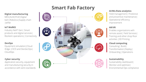
Smart Factory for Semiconductors
semiconductor manufacturing is a complicated process that requires very little human interaction. One example is the manufacturing of wafers, a thin slice of semiconductor substance. This process must be extremely precise and cannot tolerate any particles such as hair or skin falling onto the wafer and damaging the chips. To put it in perspective, a 5-nanometer chip is equivalent to about 1/1000th of the diameter of a human hair, so even a speck of dust could cause collateral damage. That said, current iPhones use 5-nanometer chips, so you can imagine how precise the process needs to be.
Smart Factory is a solution suite that seamlessly spans on-premises and cloud-based Manufacturing 4.0 capabilities. Transform Semicon manufacturing business through insights and intelligence powered by data integration, the Industrial Internet of Things (IIoT),Data analytics AI/ML, PLM, AR/VR, could computing, sustainability and predictive analytics. By bringing together the digital world with the physical world of manufacturing, Proficy Smart Factory can deliver holistic performance management for today’s connected enterprise.
Artificial intelligence/machine learning (AI/ML) & IoT has the potential to generate huge business value for semiconductor companies at every step of their operations, from research and chip design to production through sales.AL/ML & IoT has been a major catalyst for the semiconductor industry to generate business and extract economic value at every stage, from operations to design to fabrication to R&D to manufacturing to sales and even the supply chain.
AI helps modern wafer inspection systems automatically detect and classify defects early in the production process and with very high accuracy–even better than human inspections.
Deploying ML algorithms help identify patterns in component failures, predict likely failures in new designs, and propose optimal layouts to improve yield.
Robotic handling of wafers can reduce contamination and deliver cleaner wafers for subsequent processing steps. The reduced size of features in semiconductor microstructures means that a single particle can block etching of a key feature or impact doping in a critical part of the semiconductor component. It is vital to keep contamination of wafers to a minimum, and robotic handling of wafers reduces the sources of particle contamination.Robots are also used increasingly in the meeting and testing of silicon wafers in the course of manufacturing semiconductors.
IoT technology will play an important role. Throughout the chip manufacturing chain, IoT applications are used to monitor quality, inventory control, device tests, packaging, and delivery. IoT makes preventative maintenance of equipment and predictive analysis of processes throughout the manufacturing process possible.
Digital twin contains all the information of the physical system, it’s reflect performance in real-time. Information flow back to the digital twin from the actual results from MES, maintenance, test and scheduling.
Operations managers can use mixed or virtual reality (VR) glasses to interact with a digital twin, which shows exactly what’s happening on the factory floor at any given time — and which production adjustments are possible. With a digital twin, they can immediately pinpoint quality and safety problems; monitor machine capacity, material in stock and workflow; make changes as needed; and program factory-floor machines to know when to make the changes themselves
All semiconductor companies (fabs, fabless, IDMs, foundries, OSATs/subcons, and photonics) can use the latest end-to-end product lifecycle management (PLM) software to reduce time to market (TTM). They conquer product complexity, react to changing requirements at the speed of business and gain insights to predict future product needs.By implementing PLM, semiconductor companies can realize significant benefits, including a centralized, single version of the truth for all product data; improved collaboration, control and communication of product design, development and engineering change order information; improved chip quality, design, development productivity and manufacturability of ICs; enhanced design and elimination of rework by enabling input from multiple parties early in the product development process; reduced cycle times and time-to-market through standardization of processes and tools, etc. With industries slowly transitioning into digital enterprises where all the processes such as product design, manufacturing processes, services & support, and customer experiences are connected via a digital thread, PLM solutions offer the foundational structure and framework for implementing the digital twin, which is fast becoming an integral part of the overall digital transformation.
Sustainability:
Rising energy demand while optimizing energy efficiency and reducing CO2 emissions, can be achieved by reliable data, collected by sensors. Interpreted correctly they can lead to energy savings by uncovering inefficient production flow, optimizing production and logistics planning, and anticipating maintenance needs.
Edge AI is an emerging field and growing fast. Edge AI can combine the power of the cloud with the benefits of local operation to improve the performance of AI algorithms over time. The original paradigm of simply moving all of the data generated on the edge to the cloud for analysis and machine learning has run into three fundamental barriers, namely privacy, reliability and latency. Running these algorithms efficiently on edge eliminates these barriers and allows AIoT products to scale much more rapidly. Powerful semiconductor solutions from Infineon create the framework for IIoT at the edge:
Edge AI enabled MCUs help to identify at-risk equipment, repair urgency and control adaption
Smart actuators receive and implement instructions to reduce potential impacts in production
Security solutions ensure secured communication and protection of critical information
Connectivity technologies enable dependable communication across devices, factory levels, cloud and secure device management.
Smart Factory provides the tools to successfully transition to a digitally driven model:
- Track data across plants, equipment,materials, and people
- Specify metrics to track across allyour equipment
- Use intuitive browser-based, out-of-the-box screens as a digital cockpit for fast time to value
- Create custom views within role-specific dashboards
- Create the necessary visibility to quickly generate a new bill of materials, reroute components, change equipment schedules, and re-assign employees appropriately
- Monitor production and catch deviations and make adjustments to avoid wasted materials
- Predict overruns and shortfalls before they happen then reschedule your orders to optimize based on material, equipment and personnel availability
- Understand your operations better with traceability across the entire scope of the production process
- Leverage innovation best practices
- Achieve 30% lower Total Cost of Ownership (TCO) through cloud
 Summary
The digital transformation within the Semiconductor industry to continue and accelerate. Nearly three out of five chip companies have already begun their transformation journey. Still, over half of those are modifying their transformation process as they go, in response to disruptive forces reshaping the Semiconductor Industry.
The impact of these disruptions creates a need for new capabilities e.g. Agile Operations to accelerate business Value, Virtual Enterprise to improve flexibility and accelerate responsiveness, AI-enabled inventory, planning, and supply chain processes, AI-enabled Knowledge Management,Data platform, governance, and AI application DevOps & Intellectual Property analysis and advisory tools. etc.
Major Semiconductor chip manufacturers found that bringing disparate systems and processes into a holistic MES solution integrated with ERP delivered substantial benefits. First, it forced them to organize the information and enforce protocols which, in turn, created better understanding and continuous improvement to meet complex semicon process requirements. Having previously used legacy MES technology to guide shop floor processes, the new MES provided much-needed increases in granularity to drive efficiencies. First pass yield increased and chip manufacturing cycle times decreased; there was also a beneficial information flow increase, greater visibility into processes and error reduction. Overall, the impact on the bottom line was significant. But perhaps more importantly for the future, the investment made today in a fully scalable MES offers this customer even more ways to reduce production costs and increase production capacity through legacy equipment integration and even tighter parameter control while enabling future expansion. Essentially, the customer gained a much more productive present day production environment as well as easier pathways for future expansion.
It turns out that the path to the smart semiconductor factory is feasible and offers various advantages to the Semicon Chip manufacturer. The move to the smart factory is becoming increasingly important for competitiveness and customer relationships.
About the Author :

Mr. Shivam Mhapankar PMP ® ITIL ®
Sr. SAP Program Manager (SAP S/4 HANA/Cloud Managed Services for SAP)
IBM Consulting
![]()
Shivam is the Sr. S4 HANA Program Manager & Business Development Executive for the Hi-Tech Industry, for IBM consulting – CIC India.
He has a 20+years track record driving innovation and changes in the Electronics Industry in supply chain operations, information technology, and enterprise business transformation to enable profitable revenue growth. He has broad-based strategic, business, consulting, and project management skills gained over years of experience in the industry.
Mr. Shivam Mhapankar can be contacted at
Mobile : + 91-99308 61764
E-mail: [email protected], [email protected]
LinkedIn : shivam-mhapankar-9a79731b7


